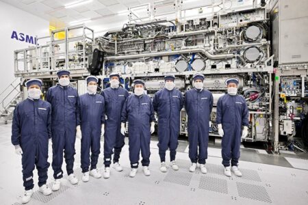
SK Hynix announced on Monday that it began producing 10-nm 8GB LPPDR4 mobile DRAM this month. The South Korean giant added that it was applying the extreme ultraviolet process in its production of the latest chip.
The latest chip is the first time that SK Hynix has applied EUV in its DRAM production. Samsung began using the process last year and Micron says that it is planning to apply the process in 2024.
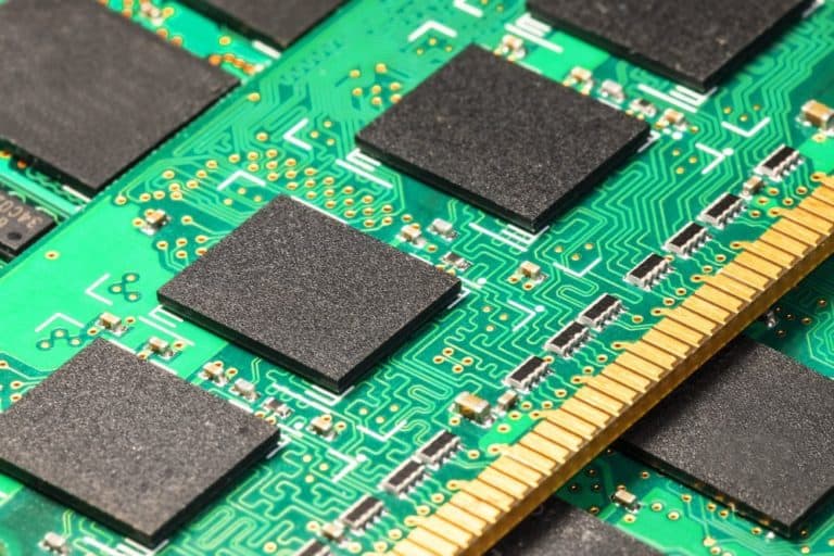
EUV equipment is used in the lithography process of chip production where the circuit patterns are transferred onto the wafer.
More efficiency
Using EUV, the chip makers can transfer more precise patterns that allow the chips to be designed smaller and to have more of them be drawn on the wafer. Besides memory in logic chips, the process is seeing wide adoption by Taiwanese Semiconductor Manufacturing Company and Samsung, in their advanced processor production.
SK Hynix said that the application of EUV allowed it to secure 25% more units of DRAM in one wafer, for its latest 10nm LPPDR4, than its predecessor. The company also reported that the DRAM would also help alleviate the supply and demand conditions in the global market.
What SK Hynix is planning
All of SK Hynix’s new DRAM products with the 10nm process will be made using EUV going forward. The South Korean company also released details about the specs, saying that the LPDDR4 mobile DRAM runs at 4,266 Mbps and uses 20% less power than its predecessor.
SK Hynix reported that the chip will be supplied to smartphone manufacturers in the second half of 2021. The company will start applying the latest 10nm process to its DDR5 production starting next year.