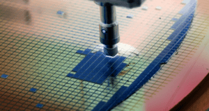
IBM has created materials and processes that can help improve the efficiency of the production of 7nm and smaller chips. That’s what ZDNet reports. This is intended to transcend the limits of chip development.
Big Blue researchers are working on challenges in the emerging field of area-selective deposition. This is a technology that can help overcome limitations in lithographic techniques to make patterns on silicone in the 7nm process.
Techniques such as multiple patterning helped to ensure that integrated circuits could continue to scale. But when chips shrunk from 28nm to 7nm processes, chip manufacturers had to process more layers with ever smaller functions that were placed on patterns in more precise places. These functions must connect between the layers. If not, it leads to edge placement error (EPE).
Yan Borodovsky, lithography expert at Intel, thought this problem could not be solved by lithography and would eventually mean the end of Moore’s Law. In 2015, however, he encouraged the industry to investigate area-selective deposition, which is what IBM researchers are doing now. This could possibly be the successor of EUV lithography, the technique Samsung is currently working on.
Solution
Area-selective deposition requires a tool that can place different combinations of materials on a device. For example, it concerns metals on metals. “In traditional development methods, you have to coat a substrate with a resist, place the resist through an exposure step, develop the image, deposit an inorganic film and then strip the resist to give you an inorganic material with a pattern,” says Rudy J Wojtecki, researcher at IBM’s Almaden Research Center.
“We’ve found a way to make this inorganic film easier to deposit, with a process that automatically streamlines it. In doing so, we immerse a patterned substrate in a solution containing a special material, and add that substrate to a landfill chamber. Then you’re done. We are literally able to make a component of a device in a controllable way at the nanoscale.”
The technique may be able to help develop hardware that better supports AI applications.
This news article was automatically translated from Dutch to give Techzine.eu a head start. All news articles after September 1, 2019 are written in native English and NOT translated. All our background stories are written in native English as well. For more information read our launch article.