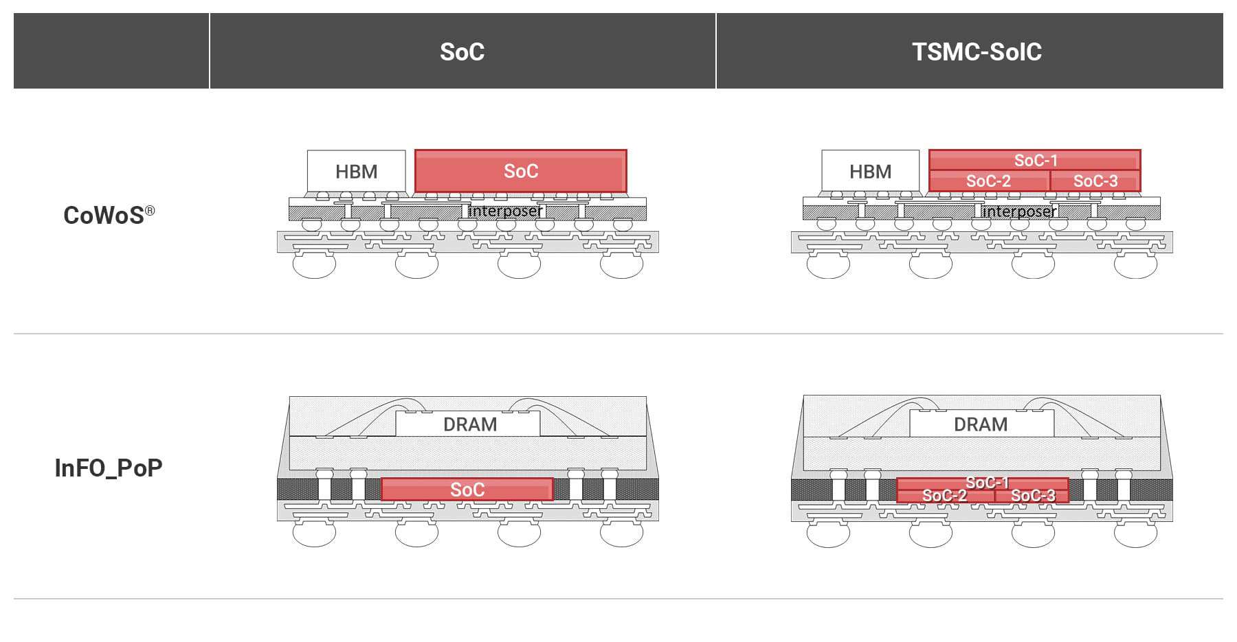
Taiwanese chip manufacturer TSMC is working with Google and AMD on a new technique to create 3D stacked chips. By packaging different parts of a chip on top of each other, the chips should become more compact and efficient.
The rumour about the collaboration originates from Nikkei Asia. The paper writes that, as Moore’s Law is becoming increasingly difficult to keep up with, companies are looking for new ways to keep progress going other than focusing on further reducing process nodes.
Different packaging
With the new developments, the companies focus on the way the chips are packaged before they are placed on a circuit board. According to Nikkei, this step was not known as a very complicated one, but apparently, there are performance gains to be made by taking a different approach to this step.
Stacking
The plan is to stack different types of chips, such as the processor, memory and sensors on top of each other. These components are often integrated into a single chip, but in most cases, they are positioned next to each other. With this new approach, the chips should become smaller, more powerful and more efficient.
2022
TSMC calls the new 3D stacking technique SoIC, which stands for System on Integrated Chips. The first customer for the technique is AMD, sources tell Nikkei. TSMC is building a factory for this purpose in the Taiwanese city of Miaoli. The factory should be ready in 2022.
Tip: TSMC accelerates production process 5 nanometer chip due to 5G introduction