When Chinese chipmaker SMIC ordered an ASML EUV machine in 2018, the US government intervened to block the sale. Five years later, amid a relentless tightening of export controls, then-ASML CEO Peter Wennink warned of an inevitable backlash: China would be forced to develop the world’s most advanced chipmaking technology on its own.
That warning is now becoming a reality. A working prototype has reportedly emerged in Shenzhen, the product of a Chinese ‘Manhattan Project’, a nod to the frantic WWII race to build the atomic bomb. Just as American-led scientists, many of them refugees from occupied Europe, outpaced both Nazi Germany and their own Soviet allies to master nuclear fission between 1942 and 1945, Beijing aims to bridge the gap in semiconductor between theory and practice with similar speed. If successful, Chinese EUV-based processors could debut as early as 2028, marking the first time such chips are produced entirely independent of ASML’s headquarters in the Dutch town of Veldhoven.
Former ASML employees
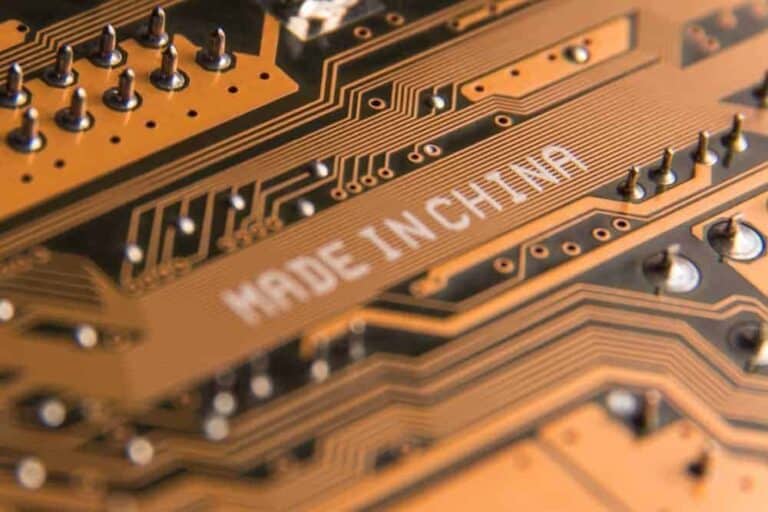
ASML delivered its first EUV lithography machine in 2010, though it was still a prototype. EUV lithography, short for Extreme Ultraviolet, has only been viable for mass production since 2017-18. Currently, EUV machines are exclusively operated in Taiwan (TSMC), South Korea (Samsung), and the US/Europe (Intel). These are massive, energy-intensive, and incredibly expensive systems, but their unparalleled precision, achieved by lasers operating at the far reaches of the light spectrum, makes them indispensable for the most advanced chips. China, and specifically its national champion SMIC, has never been granted access to them. Instead, it relies solely on DUV machines for mass production and, following Dutch and US export bans, is now even barred from purchasing the latest DUV models from ASML, Canon, or Nikon.
We have previously covered China’s efforts to circumvent these barriers. By pushing DUV equipment to its absolute limit, SMIC approached the 7-nanometer node, a threshold typically reserved for EUV. While the resulting Huawei Kirin 9000S chip was not particularly impressive compared to its global peers, the methodology behind it was: it cleverly sidestepped the inherent constraints of DUV. However, clever tactics cannot bend the laws of physics; the sharp focus of the extreme ultraviolet spectrum has no true substitute in DUV technology.
This limited breakthrough signaled to the world what Beijing likely already knew: China had to build its own EUV ecosystem. Former ASML CEO Peter Wennink warned of this exact scenario: ‘You are forcing them to become very innovative,’ he told Nieuwsuur in September 2023. ‘They are coming up with solutions that we haven’t thought of yet.’
What he may not have known, but likely suspected, was that some of his own former staff members would facilitate this push. According to two Reuters sources, former ASML engineers assisted in reverse-engineering EUV lithography. This step seemed almost inevitable, as the bespoke solutions developed in Veldhoven cannot be easily replicated. While the principles of EUV lithography are rooted in the laws of nature, only ASML has mastered the engineering required to turn those principles into a functional product, a feat even Japanese rivals Nikon and Canon never managed to achieve.
‘Many, many years’
Wennink’s successor, Christophe Fouquet, offers a slightly different perspective. In April, the new ASML CEO spoke of China needing ‘many, many years’ of research and development to produce a viable alternative to ASML’s technology. The recent Reuters report sheds light on exactly how long that might be. While the prospect of functional chips by 2028 may be an optimistic projection of Chinese progress, 2030 appears increasingly realistic.
The objective is unmistakably clear. Sources indicate that President Xi Jinping aims to purge American—and by extension, Western—influence from the entire semiconductor supply chain. The current working prototype is the culmination of six years of intensive state-led investment aimed at securing this independence.
To maintain secrecy, the former ASML employees involved were reportedly issued identification cards with aliases, alongside substantial signing bonuses. Much like the original Manhattan Project, every milestone was treated as a state secret. The team is said to include recently retired Chinese ASML engineers, who possess the specialized expertise required to execute what is perhaps the most ambitious reverse-engineering project in history.
China’s primary advantage is its ability to pour ‘many, many yuan’ into this effort for ‘many, many years.’ Should the prototype eventually evolve into a mass-production machine, any initial inefficiencies could likely be offset by near-infinite state subsidies. The fundamental hurdle, however, remains the supply chain. An EUV system is only as good as the components provided by a global network of specialized suppliers—many of whom, like Carl Zeiss and its world-leading optical systems, hold a virtual monopoly on the necessary technology. In this regard, China must do more than just build a machine; it must replicate ASML’s entire ecosystem.
The real gap
These reports are alarming for US policymakers intent on curbing China’s technological rise. However, the exact extent of China’s progress remains obscured. While it is known that ASML once offered to monitor activities in China for the US, and previously discovered a Russian spy within its own ranks, Reuters notes that former employees represent a significant blind spot; ASML simply lacks the authority to track its alumni. The reported involvement of Lin Nan, ASML’s former head of light source technology, in this new ‘Manhattan Project’ serves as a stark example of the critical expertise now bypassing Veldhoven.
Experts point out that China is not starting from zero. Unlike ASML in the years leading up to 2010, the Chinese already have proof of concept: they know EUV lithography works on a commercial scale. With former engineers potentially sharing their blueprints, the primary uncertainty shifts to the supply chain. Can China fully replicate the web of highly specialized suppliers that make an ASML machine possible? If they can, the obstacles shift to operational reality. The energy requirements for EUV are staggering—even more so for High-NA EUV, the industry’s latest frontier. While ASML has lived and breathed this technology for fifteen years, its official response remains characteristically brief, calling any attempt to build an EUV alternative ‘no small feat.’
Reaching this stage is indeed no small feat, but the true test lies ahead. It is becoming increasingly clear that China will one day produce advanced processors without ASML. While their ambitions are vast, the specific challenges remain largely unknown and their current progress is, at best, vague. The lack of functional chips to date is unsurprising, but if they succeed before 2030, Fouquet’s ‘many, many years’ will suddenly seem like a very short window.
Currently, China appears to be occupying the developmental space ASML moved through between 2001 and 2010. ASML built its first working prototype in 2001; by 2010, TSMC received the first commercial system. We can expect China to bridge that nine-year gap much faster, fueled by the expertise of former ASML staff and decades of global scientific progress. The subsequent leap toward mass production, a milestone ASML hit in 2017, will likely be compressed as well. Then begins the race to catch up with High-NA EUV. By that time, Veldhoven will have moved the goalposts once again. Ultimately, for China, it is no longer a question of if they will succeed, but when.
Read also: ASML: from a leaky shed to the chip industry’s key player