Last year, Huawei took a big step forward in the smartphone world. Their flagships continue to innovate and the Kirin chips are becoming increasingly powerful. According to sources, this year the world’s first mass production of EUV chip is expected to roll off the production line under the name Kirin 985.
Extreme Ultra Violet or EUV is the holy grail in the world of chippings. Intel has been working on it since 2000 and still does not have an EUV process ready for mass production. The next reduction to 10 nm is planned for the end of this year, but 7 nm EUV does not yet have a deadline at Intel.
Samsung is already ahead of Intel with risk production of 7 nm EUV. To date, it is not yet known which first mass production chip will roll off the conveyor, but Samsung is on the heels of TSMC in terms of development speed.
Risk production
TSMC, like Samsung, is today already producing risk of 7 nm EUV, but seems to be gradually satisfied with the returns. WCCFTech reports that Huawei would be the first manufacturer to use TSMC EUV chips commercially in future smartphones.
The first chip to be introduced is the currently unknown Huawei Kirin 985. Possibly this is the successor of the current Kirin 980 that is in the Huawei Mate 20 Pro today. At the end of last year, Huawei was already the first to launch a 7 nm chip at IFA in Berlin. It would therefore come as no surprise to us if Huawei were once again to want to show off the EUV premiere.
The current 7 nm process of TSMC is called N7. The EUV variant is called N7+ and is 10% more energy-efficient according to sources. Thanks to EUV, transistor order can also be increased by 20%.
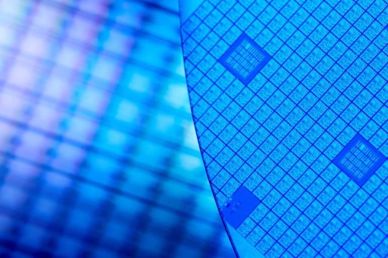
Why EUV?
Today, everyone uses an Argon Fluoride (ArF) laser that produces a deep UV light with a wavelength of 193 nm. Thanks to a technique called immersion lithography, they can increase the resolution, but today they have to go through some complex functions in several steps. EUV lithography generates light with a wavelength of 13.5 nm.
EUV has many advantages. This gives you a better result in terms of pattern efficiency and less variability in dimension. In short: what you print is what you actually get. Samsung claims that the new tools deliver 70 percent more correct patterns compared to the 193 nm ArF tools.
The most important thing, however, is the budget savings brought about by EUV. At 7 nm, the machine can handle contacts and certain metal layers in one step, while at 193 nm ArF requires multiple exposures.
Related: How EUV lithography causes a musical chairs dance in a processor country
This news article was automatically translated from Dutch to give Techzine.eu a head start. All news articles after September 1, 2019 are written in native English and NOT translated. All our background stories are written in native English as well. For more information read our launch article.