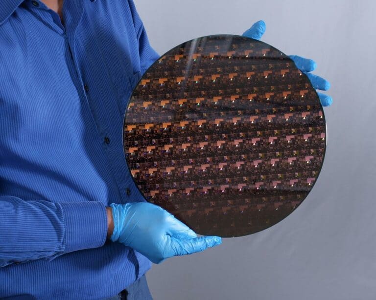
IBM has built the first wafer with semiconductors on the 2nm process. The successful test is an important step towards making chips smaller, faster and more power-efficient.
The processor on 2 nanometres should perform 45 percent better with the same power consumption as a comparable processor on 7 nanometres. For the same performance, power consumption will be 75 percent less, according to IBM. A fingernail-sized chip can accommodate 50 billion transistors.
AnandTech asked IBM how big an IBM fingernail is and was able to ascertain that IBM has managed to produce 333 million transistors per square millimetre. That is considerably more than the smallest processes that competitors TSMC, Intel and Samsung are currently working on.

EUV exposure
To get the transistors so small, IBM uses the EUV exposure process on a 300-millimetre silicon wafer. A new technique called Gate-All-Around is used to design the transistors. This makes it possible to stack three transistors on top of each other.

Collaboration with other companies
This milestone was reached in the IBM Research laboratory in New York, in cooperation with the State of New York, Samsung Electronics and Intel. IBM itself has no chip factories since it sold its factories to GlobalFoundries. Now IBM is working with other companies to advance the development of chip fabrication.
Commercial applications in 2024
Production of this new 2nm technology is expected to start in 2024, says Mukesh Khare, VP of hybrid cloud at IBM. According to IBM, the technology will be used to accelerate applications in artificial intelligence, edge computing and autonomous systems, among others. It will be found in systems like IBM Power Systems and IBM Z. Presumably, the technology will eventually trickle down to smartphones and computers in your workplace.
Tip: TSMC announces massive investments into chip production