TSMC’s core message at its own Technology Symposium in Amsterdam is that it will act upon the chip sector’s wishes. That wish, at the moment, is to expand globally. The Taiwanese chip giant’s reach is greater than ever, all while constantly pushing against the limits of nature.
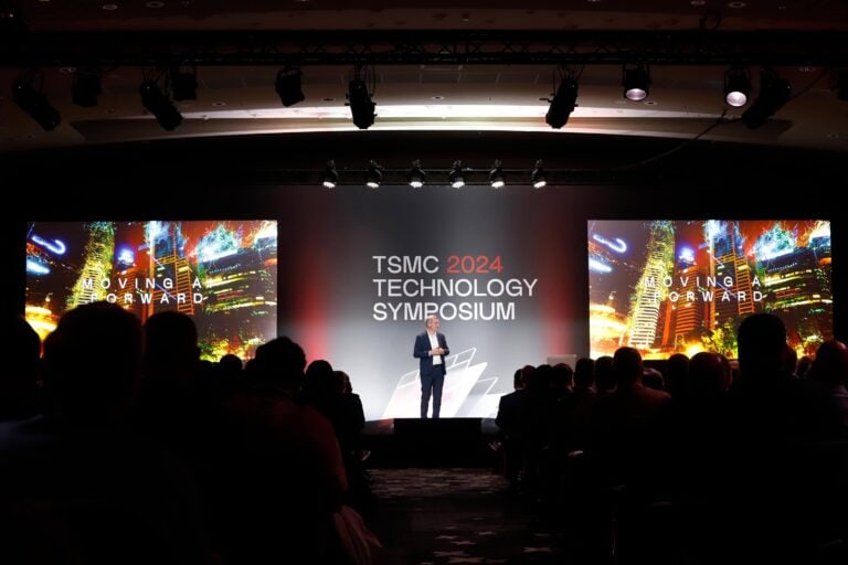
The TSMC Technology Symposium is a curiosity cabinet of tech companies. TSMC, the eighth most valuable company in the world, is joined at this event by partners big and small, from Infineon to Raspberry Pi. They share one similarity: they all have their semiconductors built by TSMC, along with the likes of Apple, Nvidia, AMD, automotive suppliers and many others. Even competitor Intel, which has its own chip factories, is partly outsourcing production of its brand-new Lunar Lake to TSMC. A total of 150 new products are being made at TSMC this year, considerably more than last year’s total of 120. Those products, as mentioned, vary considerably and see the light of day on a variety of formats. Techniques that may have been state of the art in 2008 can now be used for somewhat simpler chips or chip parts.
Tip: ASML now has second highest market cap in Europe
Growth, growth, growth
Needless to say, the AI hype has not escaped TSMC. CEO C.C. Wei jokes that you basically have to throw out any computer that cannot be called an “AI PC.” It has faced overflowing demand on several occasions and in the past 12 months, it has been the biggest bottleneck for releasing AI hardware from Nvidia into the wild in particular. As a result, prices per GPU have soared to unprecedented levels, as did the latter’s market value to three trillion dollars at the time of writing. TSMC also has the financial wind in its sails: on the Taipei Stock Exchange, its market value has risen more than 50 percent since the start of 2024.
Consequently, the Symposium has grown significantly and its speakers are telling a significantly less technical story than in 2023. Whereas the precise details of 3D interconnects and chip stacking dominated last year, it is now about a “fourth industrial revolution” fueled by AI (the previous three ran on water and steam, electrification and mass production, and computerization, respectively). The narrative is broader, more ambitious and a bit further removed from the minutiae of semiconductors than it was before.
At the event, there’s also a focus on the physical growth of TSMC itself. This expansion is needed in part because of the aforementioned surge in demand for AI chips. A “megafab” in Arizona, USA and a facility for older chip processes in Dresden, Germany get most of the attention. However, there is also expansion in Taiwan itself and just across the pond in Japan. All facilities will run on a standardized model, which TSMC describes as a “GIGAFAB” (capital letters included). This includes precise requirements for quality control and the availability of remote expertise via augmented reality and virtual reality. As a result, the entire world is effectively one TSMC chip factory, which the company makes as a not-so-subtle reference to when its presentation screen transforms the Earth’s globe into the round TSMC logo.
Challenges for all
In a way, the rise of AI is extremely badly timed. Just when everyone and their dog points to 2030 as the year to become carbon-neutral, AI calculations cause a big increase in energy and resource use. Given the highly emissive industry in which TSMC operates, it originally had the year 2050 in mind to get to net zero. Now that has been clawed back all the way to 2040, as it says progress is faster than previously thought.
Reading tip: ASML expansion agreement will be based on trust and that worries Eindhoven
TSMC obviously wants to run its own factories as efficiently as possible, but it may even have a net positive impact on the immediate environment. The Japanese location is said to return more drinking water to the region than what it takes in. When asked, TSMC reveals that similar plans are also possible for the proposed Dresden plant, as Kevin Zhang, SVP Business Development & Overseas Operations Office, highlights.
Certainty
Construction of that German plant will begin in the fourth quarter of this year. ESMC (European Semiconductor Manufacturing Company) is a joint venture between TSMC, Bosch, Infineon and NXP. That roll call may already tip you off with regard to the new fab’s purpose. Namely, Dresden’s fab will not revolve around the production of brand-spanking new iPhone and Nvidia chips, but silicon intended for use in cars and industrial settings. Hence, the chip processes here are N28, N22, N16 and N12, many times larger and older than the production processes for the most advanced chips. State-of-the-art chip parts, by the way, are actually being put in cars, but they’re not going to be built in Europe anytime soon. True European autonomy will not be available to the continent when it comes to chip production, then.
We are told by Zhang that a chip factory’s end goal can always be shifted. In this case, TSMC’s leadership is responding to the desire from Brussels to guarantee their own supply of semiconductors. As far as Germany is concerned, that mainly means securing auto parts, but so as far as TSMC is concerned, that target audience can (and may) shift if necessary.
TSMC intends to keep the latest processes within its own borders. A bold question during the Symposium: what if China invades Taiwan? What will then happen to TSMC and its factories on the island? It already became clear a little while ago that the chipmaker and its partner ASML have ways to remotely disable their systems. Zhang assumes the same principle that his TSMC colleagues have already talked about: without the chip recipe, any chip kitchen is useless. That expertise might be transferable to Arizona or Dresden, but for now, that is (thankfully) out of the question. ASML’s EUV machines are currently still running at full speed at multiple locations in Taiwan.
High-NA EUV doubts
Speaking of ASML, that company’s latest plaything, a High-NA EUV scanner called the TWINSCAN EXE:5000, is now on sale. Intel went full steam ahead with it after missing the boat with EUV technology, the previous major paradigm shift in the chip sector circa 2015. For a few months, TSMC seemed to be making a similar mistake. At the Symposium, Zhang explains, “The driver’s experience is just as important as the performance of the car.” Notably, the efficiency leaps in EUV are already significant. Since its introduction, TSMC has more than quadrupled chip yields on EUV, reduced defect rates eighty-fold, and extended the life of various components by 4x.
Read more: TSMC doesn’t need latest ASML machine yet
Yet TSMC CEO C.C. Wei recently secretly trekked to Veldhoven, Netherlands, to knock on ASML’s door. It is now clear that ASML will deliver a High-NA EUV machine, worth about 350 million euros, to TSMC before 2024 is out. Anyone looking at Intel’s miss of nearly a decade ago and seeing how long it has taken that company to become truly competitive again may breathe a sigh of relief on behalf of TSMC.
In fact, Intel can already count on Microsoft as a customer, while Nvidia is also watching with interest to see how this TSMC alternative develops. Nvidia previously used Samsung for GPU production when it couldn’t get what it wanted at TSMC in 2020, but that was a one-off. With Intel back in the serious innovation game and realizing smaller and smaller chip processes, TSMC cannot afford to fall behind. That wouln’t fit with the two pillars the Taiwanese company insists on, explicitly and implicitly: predictability and leadership in innovation.
Into the future
In the short term, as mentioned, things look good for TSMC. However, several sectors and regions are healthier than the others. For example, the chip industry worldwide shrank eight percent, while the EMEA region remained stable. TSMC proclaims “mixed momentum” in 2024, with 2023 having been a correction year for chip makers. Demand for AI hardware rolls on, there is a mild recovery in smartphones and the PC sector, but automotive and IoT is somewhat “soft.” The bottom line: structural growth is still strong, according to TSMC, especially since its industry has always assumed longer-term undulations. The fact that the average annual growth rate in the EMEA chip sector since 1997 sits at 14 percent offers hope in that regard.
Long-term, efficiency is going to be the name of the game for TSMC and its competitors. This isn’t only in regard to its own operations, but primarily when it comes to the semiconductors it produces. Where the human brain easily exceeds the computing power and complexity of modern semiconductors, it does so with only 20 watts. A move toward such efficiency seems like science fiction, but it will eventually be necessary. After all, if we’re not careful, data centers consume seven percent of the world’s electricity. At TSMC, musings about”neuromorphic processors,” chips with synapses like human brains have, have now reached the public stage. It’s a somewhat striking suggestion, especially since the small show floor even has such a processor from the Dutch company Innatera. That product, however, is a presence detector, an impressive feat of engineering especially with such an esoteric design, but clearly far away from the human-like intelligence TSMC is hinting at.
Also read: NXP and Taiwanese VIS invest 7.8 billion in wafer plant in Singapore
We also hear at the TSMC Symposium that other materials should be considered for chip production. Silicon and copper currently form the basis for chips and interconnects, but the use of gallium nitride and photonic communication within semiconductors should increase substantially in the long run.
In the somewhat shorter term, TSMC is looking ahead to N2, also called the “2-nanometer” process. No measuring point within the process corresponds to that number – it is just a marketing term. However, it is indeed smaller than N3, which the iPhone 15 series was made on, or N3P, which Intel Lunar Lake uses. The yield rate is already 80 percent, even now, with N2 not being deployable until the second half of 2025. That is a particularly high number at this stage of development. If Apple’s preferred role continues as the first to land a major deal on a brand-new process, an eventual iPhone 17 might be the first mass-market product to use N2. N2P will be a further development of this and will appear in 2026. Nevertheless, N3 will continue to be “milked”, as mentioned in the Symposium keynote.
This will be followed by the so-called Angstrom era, the yardstick that is one step smaller than nanometers. At Intel, the first of these processes will be 18A, on which Panther Lake, intended for laptops in 2025-26, will run. TSMC puts the A before the number (and they kindly ask you to do the same when asking about it) and is going to offer A16 over the next few years. It promises to be 20 percent more efficient and eight percent faster than N2P. This will mainly come from backside power delivery, a method that, for the first time, is going to offer power to the chip through the back end. Previously, this has always been on the front end, which has its space constraints. Such steps are necessary today to achieve further improvements in chip designs. After all, in the long run, there are simply too few atoms to shrink any further. With Intel also competing at the sharp end again, the drive to keep improving is greater than ever. That challenge seems to be welcomed by TSMC.
Read also: Imec raises 2.5 billion euros for test line for advanced chips