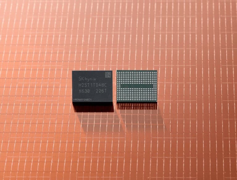
SK hynix launched the world’s first 238-layer 512GB TLC 4D NAND flash chip. This NAND chip should deliver greater productivity, higher data speeds and more power efficiency.
SK Hynix manufactured the 238-layer 512GB TLC 4D NAND flash chip using its 4D manufacturing process. The process ensures that the chips have a smaller cell area per unit compared to 3D production technology.
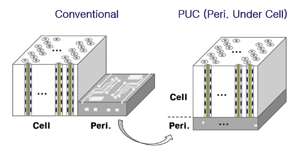
The 4D production process uses charge trap flash- and peri under cell production technology. Ultimately, the 4D technology should yield more efficient production.
Technological advantages
The new NAND flash chip is the smallest NAND chip currently available. The smaller the chip, the more chips can be fitted on a wafer during the process.
Furthermore, the 238-layer chip yields a higher data transfer rate than other NAND chips. SK hynix clocked the speed at 24 Gbps, up 50 percent from the previous generation of NAND flash chips. Furthermore, the energy consumption for data reading was reduced by 21 percent.
Suitable for SSDs in PCs
According to the manufacturer, the 238-layer 512GB TLC 4D NAND flash chips are initially suitable for client SSDs used as storage devices in PCs. The chips will become available for smartphone storage and high-capacity data center SSDs at a later date.
The production of the 238-layer 512GB TLC 4D NAND flash chips will start in early 2023. Later that year, 1TB 238-layer products with double the density of the current 512GB version will become available as well.