
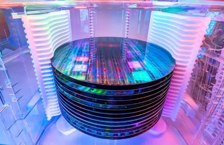
Diamond Foundry claims to be the first company to produce a single-crystal diamond 200 millimeters in diameter. The material could eventually help manage heat generation in AI chips and other high-performance semiconductors.
The U.S. company announced the development during CarbonSemi 2026 in Ningbo, China. CEO Martin Roscheisen presented the diamond via a video link. According to Diamond Foundry, this is the first time a monocrystalline diamond of this size has been produced without joining separate crystals together.
Diamond has exceptionally high thermal conductivity, about five times that of copper, which allows the material to dissipate heat rapidly. This is particularly relevant for high-performance AI processors, where increasing amounts of energy and heat concentrate in a small area. Heat generation is a major limitation to further improving the performance of such chips.
Until now, the use of diamond in semiconductors has been limited, in part, by the size at which the material can be produced. Both natural and synthetic single-crystal diamonds were typically considerably smaller than the wafers used in the chip industry.
Scaling up to industrial production
The new diamond has a diameter of 200 millimeters, comparable to the wafers processed in existing semiconductor factories. According to Diamond Foundry, production required adjustments to crystal growth, plasma technology, and reactor architecture, among other things.
The company emphasizes that this is not a wafer composed of multiple diamond crystals. The entire structure consists of a single crystal. This is important because grain boundaries can affect the material’s properties.
This development builds on approximately 25 years of research into producing larger single-crystal diamonds. Diamond Foundry cites researchers Stefan Gsell and Martin Fischer, who have been working on this upscaling for a long time.
Diamond Foundry is not the only company seeking to use diamond for cooling semiconductors. For example, in 2024, Akash Systems received U.S. government funding for technology that combines gallium nitride with synthetic diamond. De Beers and Frore Systems are also developing diamond-based cooling solutions, according to Tom’s Hardware.
Diamond’s high thermal conductivity makes it suitable for reducing local hotspots in processors. Another key advantage is that diamond is an electrical insulator. This allows the material to be used close to electronic components without conducting electricity.
No commercial application yet
Although the diameter matches a standard size in the semiconductor industry, this does not mean diamond wafers can be deployed on a large scale immediately. Furthermore, the first sample is still unpolished and is being displayed as it came out of the growth process.
For commercial application, factors such as reproducibility, material quality, processability, and production costs must be evaluated. Diamond Foundry did not provide specific details regarding production volumes or the cost per wafer in its announcement.
The company views this development as an intermediate step toward producing 300-millimeter-diameter diamonds. That size is widely used in modern chip factories. According to Tom’s Hardware, Diamond Foundry expects to achieve this size by 2030. It is not yet clear when diamond wafers will actually become available on an industrial scale.