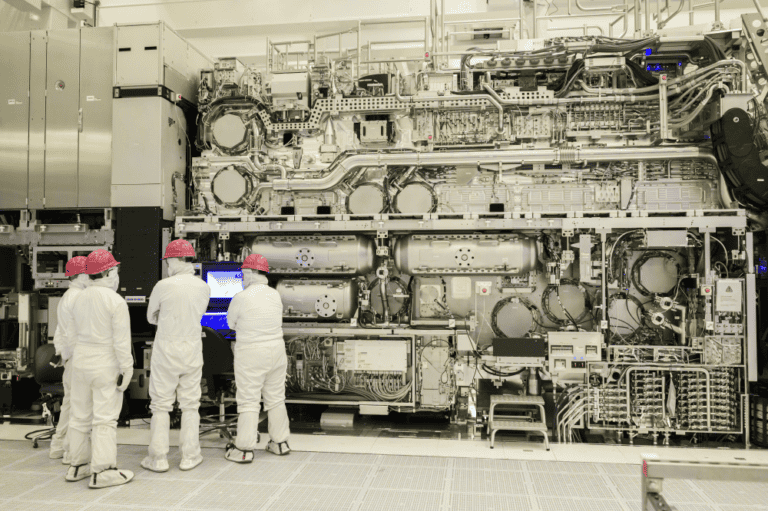
Intel has just announced that ASML’s High-NA EUV machine has finished construction. For the first time, the so-called Twinscan EXE:5000 has made 10-nanometer lines on a piece of silicon, proving that all components work correctly to some degree. The new device will enable future manufacturing processes, but first, both Intel and ASML will do considerable testing to make it happen.
Director of Lithography, Hardware & Solutions at Intel Foundry Mark Phillips explains why this development matters. The Twinscan EXE:5000 is now fully functional. All the components to make the full scanner the size of a two-story house are now installed. However, the real work has yet to begin, as a brand-new production method requires countless tests and studies.
Tip: ASML sends High-NA EUV machine to second customer
Phillips is very happy with ASML’s new instrument. While the colossus is still intended for R&D purposes, it will eventually enable chips for mass production. So, in effect, we have already seen the delivery of the world’s first “real” high-NA EUV machine in late December.
High-NA EUV
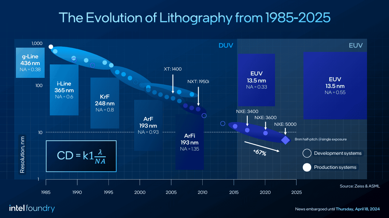
High-NA EUV refers to the latest semiconductor production method using extreme ultraviolet (EUV) light. It is the next step by ASML and its partner companies in their “constant pursuit of shrink“, in which the chip designs drawn get smaller and smaller. This time, the size of the smallest design on a chip, known as critical dimension(CD), is 8 nanometers. It is a substantial reduction from “regular” EUV, which had 13.5 nanometers as a minimum. Its predecessor DUV (deep ultraviolet) was used for the most advanced chips pre-2015. Relative to EUV, its minimum size like comparing Duplo to Lego: the smallest design it can handle is a positively gigantic 30 nanometers. For context: a human hair is about 90,000 nanometers thick.
It should be noted, however, that the very smallest dimensions are only used for certain components. Phillips tells us that only if a part of the chip is a bottleneck does it make sense to make it with High-NA EUV. In other words, relatively simple parts of a chip, such as input-output logic (in the I/O die), are manufactured using older processes. It is the advantage of the new chip manufacturing technique known as”advanced packaging,” which means that chips no longer consist of 1 piece of silicon but several, brought together by high-speed interconnects to act as a single chip.
Leadership role
There is no question that the ASML machine is very pricey. Moreover: Intel, TSMC and Samsung will need quite a few to supply their factories in America, Europe and Asia. How many of them Intel itself will need specifically, Phillips won’t reveal; Intel never shares that kind of information. But: “Every time I’ve told people the price of a new instrument, everyone was taken aback,” Phillips says. Still, it’s worth it, he believes, and Intel will know that all too well.
Read also: Latest ASML machine reaches “first light” milestone
Much, incidentally, has remained the same within the ASML design. For example, the wafer module, which holds the silicon disks on which computer chips are produced, is the same as in previous EUV machines. “ASML has gone much further than before [in terms of modularity, ed.],” Phillips states.
That makes quite a difference, especially since each device costs about 400 million euros. Being able to reuse parts ultimately means that ASML and its manufacturing partners don’t have to pass on additional development costs to customers like Intel, Samsung and TSMC. For that high price tag, customers do get something in return: an exceptionally high production capacity for such a young technology. For example, High-NA EUV machines can work through 185 wafers per hour. That’s a huge improvement over the first EUV machines from around 2015, which could process only 120 per hour.
Admitting mistakes
The “first mover” position in High-NA EUV is very significant for Intel. According to Phillips, it indicates that Intel is back as a leader in chip technology. That has been different at times: around 2015, the company under then-CEO Brian Krzanich decided to leave EUV technology for others to invest in. The company kept on using older technologies, thinking it’d be a cheaper way to success. This led to years of lagging behind competitors Samsung and especially TSMC, who did believe in EUV. When Pat Gelsinger took the helm in early 2021, one of the main targets was to claw back a process node advantage. This requires a great deal of investment, especially in the short term.
Tip: Microsoft deal and ASML tech complete Intel resurgence
High-NA EUV, a further development of this technology, will satisfy Intel’s urge to get back on the horse. Despite all the positive signs this time, Intel’s EUV fumble will have been an important lesson for the U.S. chipmaker. Indeed, it was there early on to assess with ASML certain choices in the development process. As a result, it has directly impacted the current manifestation of High-NA EUV.
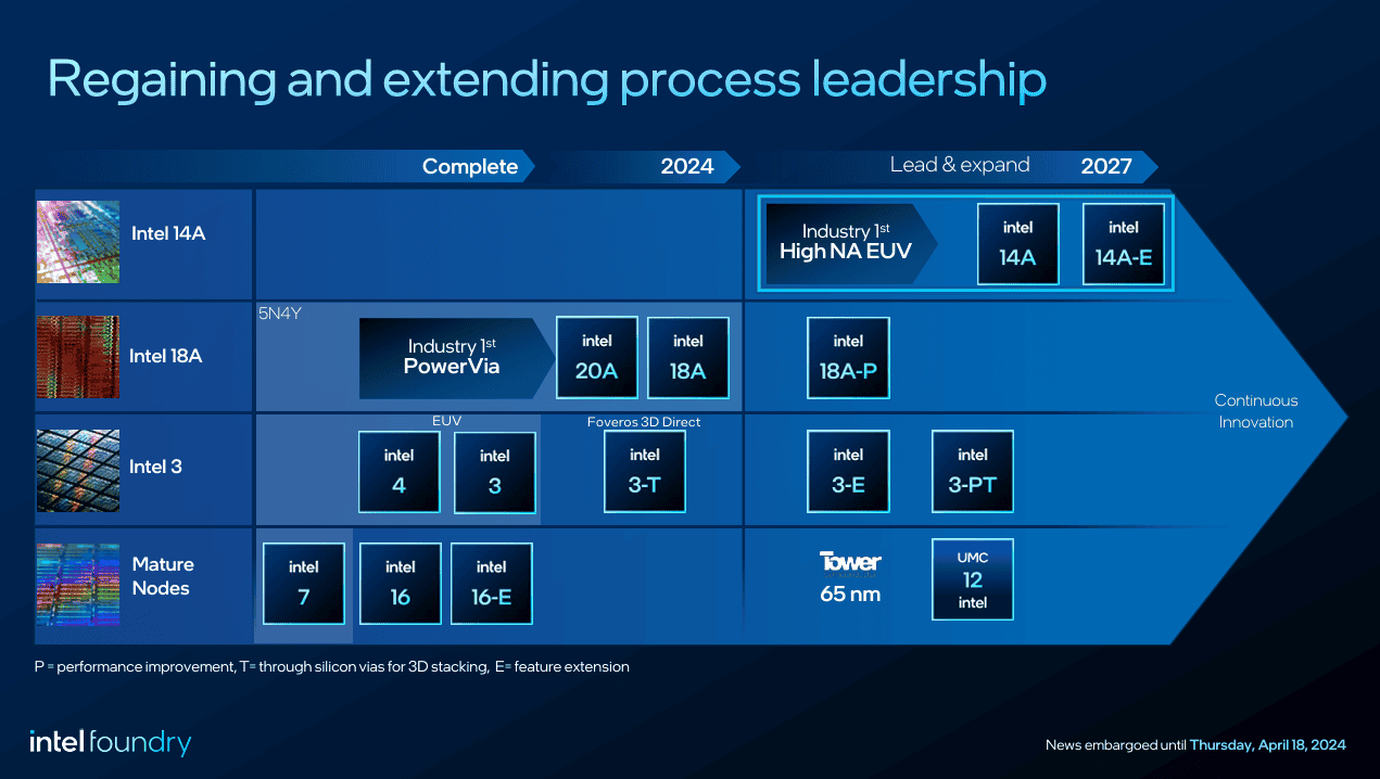
Ideally, Intel will be baking new chips on High-NA EUV starting in 2025, although, as usual with roadmaps, we’ll take a wait-and-see approach to this one coming true. The first process node intended for this technology is 14A, a few steps beyond Intel’s current portfolio. During the unfortunate period when Intel had to get by without EUV technology, it seemed permanently stuck on a chip technology that should have been obsolete years earlier. That should not be the case this time.
Built in America, and not temporarily in Veldhoven
We repeatedly refer to ASML as a ‘Veldhoven-based company’ since its headquarters are located in that Dutch village with less than 50,000 inhabitants. However, an ASML scanner is above all an international product built by thousands. That’s not only because the German company Zeiss provides the optics or American suppliers are involved, but also because ASML itself has large facilities elsewhere.
This time, the Twinscan EXE:5000 was first built in Veldhoven, after which it was taken apart and moved in pieces to America. Number two, by now already present at an anonymous customer, might never have been present in the Netherlands. With regard to Intel itself, subsequent devices could be put together directly in the US state of Oregon. This means it can push the second machine into service a lot faster.
And the future?
The fact that the EUV scanner has been built doesn’t mean too much in the short term. It does little to the stock market value of both ASML and Intel, both of which have had to deal with some recent disappointments. However, it is short-sighted to argue that some dips in stock value should worry them too much. ASML has experienced downright astronomical growth since the debut of EUV in 2015, while Intel simply has to make hefty investments in chip factories to play a leading role. The latter now hopes to make other parties’ chips through Intel Foundry as well. A deal with Microsoft is already in place, while Nvidia is also open to a possible agreement if the conditions are right.
In short, today’s announcement is a meaningful step that will prove profitable in the long run. ASML, after the current “transition year,” expects to come back strong as early as 2025, while Intel points to 2030 as an appropriate time to look forward to, when the company’s fabs are up and running and it’s pushing out state-of-the-art chips of its own as well as for its Foundry customers. Either way, High-NA EUV will play a huge role for both parties in the coming years. Current chips are at 2 and 1.8 nanometers, but with High-NA, the reduction to 0.2 nanometers can eventually be made. Reaching that target may take another ten to fifteen years. Patience, then, is required.


