Early this century, Canon, Nikon and ASML were fiercely competing for the lead in the lithography market. Over two decades later, ASML has emerged as the undisputed leader. Meanwhile, its Japanese competition dropped far behind in the R&D race. The technological gap with ASML appeared to have become nearly unassailable – at least, so it seemed. Today, Canon claims to be nearly ready to support even the most advanced manufacturing processes with its brand new equipment. Should ASML be worried?
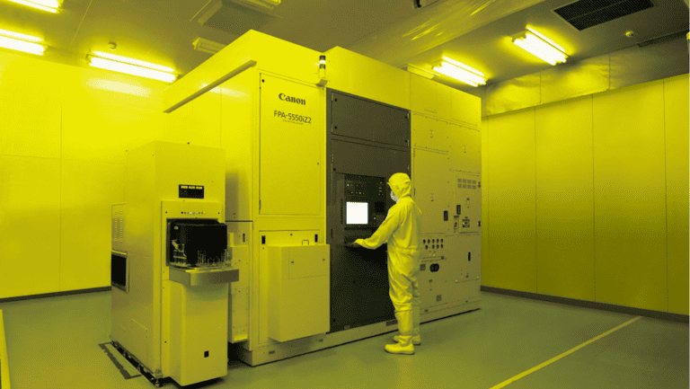
Earlier today, Canon announced that it had developed the FPA-1200NZ2C, a machine capable of manufacturing semiconductors using nanoimprint lithography (NIL). This technology imprints the design of a chip circuit onto a semiconductor wafer, “like a stamp,” as the Japanese company puts it. The new product does not require a light source at a special wavelength like ASML’s offerings do. This means that, when compared to photonic lithography, it should be a lot more efficient. To top it off, Canon anticipates that future machines with NIL technology can support manufacturing processes as small as 2 nanometers. Currently, a chip based on a 5nm design is already possible.
Canon is best known to the general public as a manufacturer of cameras and printers. However, it has had a long history when it comes to chip-making machines. As far back as 1970, it built the PPC-1, the first Japanese lithography machine for building semiconductors. Like Nikon, it grew to become one of the three biggest players in that field, although ASML outpaced its competitors from the turn of the century. Victory proved to be incredibly lucrative, as ASML is now by far the most valuable tech company in Europe. It is the sole producer of EUV lithography, which is essential for the most advanced microchips. In other words, everything from the iPhone 15 to the latest memory chips in data centers are only possible with ASML technology.
Tip: ASML to deliver the first of its revolutionary EUV scanners this year
Expertise
NIL technology has been developed by Canon since 2004, but has one major disadvantage, among others, that the yield rate is rather meagre when compared to the chip fabrication technique developed by ASML. Late last year, Canon already revealed that it had plans to construct a new revolutionary factory in Japan. As its first customer, Kioxia (formerly Toshiba’s memory division) is lined up to create NAND flash memory with NIL tehcnology.
The efficiency improvement over EUV cannot be underestimated: the equipment is said to be ten times cheaper to run. This means that even with a relatively low yield rate, there is something to be said for Canon’s offering, should mass production actually be feasible. In addition, the devices are a lot more compact.
Overcoming problems
Like ASML, Canon has had to overcome many design challenges to get to this point. To illustrate: Masaki Ogasawara, Head of Electronics Design at Canon, mentions the problem of air getting between the wafer and the “mask” (the stamp used to press the circuit onto the silicon). He compares it to putting a screen protector on your phone: a small air bubble can cause major placement errors. Margins of error elsewhere are also miniscule and barely measurable, with temperature fluctuations not allowed to go past 0.02 degrees Celsius.
Should Canon actually have made its own technology suitable for mass production, it has a sizable chance of succeeding. ASML president and CEO Peter Wennink warned last year that the Dutch company is going to face shortages of chip machines through 2024. If these shortages persist, Canon could gradually become a viable alternative. Either way, NIL technology is said to be underestimated by the stock market and Canon shares are considered “terrible underperformers.” With more positive signals such as today’s news perhaps on the horizon, that might soon change.
Also read: European Chips Act is now in force: what does it mean?