Anyone looking to produce the most advanced semiconductors cannot go without ASML. The Dutch company has a monopoly on EUV lithography, making each device cost hundreds of millions of euros for customers such as TSMC, Intel and Samsung. Japanese scientists, however, recently unveiled a breakthrough that could drastically reduce the price of EUV.
The Japanese technique was developed by the Okinawa Institute of Science and Technology (OIST) led by Professor Tsumoru Shintake. It promises to make EUV lithography significantly simpler, more efficient and ultimately much cheaper. In an ASML EUV machine, six or more mirrors direct a tiny beam of light toward the final target: a silicon wafer, the flat circle upon which modern chips are drawn with this EUV light. This takes an extreme amount of energy, with each mirror, while making the light beam more accurate, also partially absorbs it. The researchers in Japan, however, have managed to achieve a workable EUV technique with just two mirrors, resulting in a tenfold energy savings. At least, in theory. More on that later.
ASML alternatives
We have written about potential ASML alternatives before. A possible competitor can really only come from Japan. Only Nikon and Canon make similar equipment to ASML. However, these Japanese companies serve the much less lucrative DUV market – the move to EUV has simply proved too expensive due to skyrocketing R&D costs. DUV scanners, the generation of chip machines before EUV and suitable for less complex chips or chip components, are still everywhere. However, if you need an Nvidia H100, an A17 Pro for in the iPhone 15 Pro or other competitive products, the use of an ASML machine is inescapable.
Canon upset the applecart last year by unveiling its promising nano imprint machines. In one fell swoop, it might be able to catch up with ASML, seeking to erase a deficit built up over decades. The construction technique of semiconductors on these new Canon devices was described by staff as “like a stamp,” different from the lightning-fast sketches drawn by ASML devices. Either way, it will be years before its true applicability – and potential for real ASML competition – becomes apparent. Customers won’t venture into it lightly, especially since the reliability of the brand-new High-NA EUV seems to be working out remarkably well at this early stage if Intel is to be believed.
Read more: Canon deploys new chip machines to take aim at ASML’s monopoly
Challenges
Like Canon’s, the technology from Japan’s OIST is a result of overcoming multiple physical challenges. Everything from air bubbles to a lack of sharpness or an overabundance of heat challenges researchers to respond differently to the laws of nature. Shintake’s team is said to have solved two problems. First, the phenomenon of aberration, also a thorny issue in astronomy, in which an observed light source appears to occur elsewhere than is actually the case. Since this light source must track the chip at the nanometer level, any miniscule aberration cripples the overall accuracy.

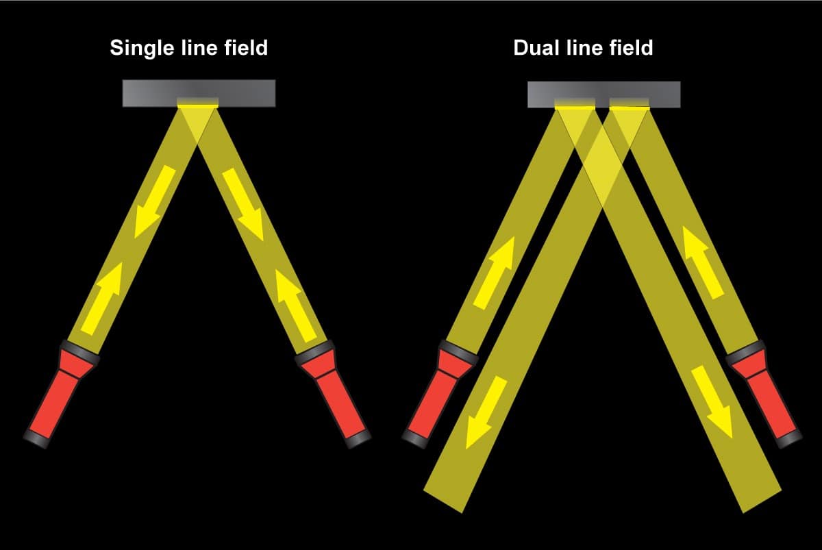
The second challenge involved light transmission. The light source often faces problematic reflections, as shown in the image above. The OIST technique hits the photomask at an angle that does not overlap with the reflection, allowing the wafer to be much more precisely exposed to light with fewer mirrors.
One problem remains to be overcome: that of reality, or actually building a machine utilizing the OIST technique. Currently, the Japanese researchers have proven the efficacy of the method in optical simulation software, but not yet in an actual machine. Obviously, it costs millions to build such a device, given that only a handful of companies can manufacture the required atomically flat mirrors, lasers and other components.
Read also: Imec shows revolution in chip technology with ASML’s High-NA EUV machines
