IBM unveiled its first chip with AI inferencing acceleration, named Telum. The chip will allow users to conduct tasks like fraud detection while a transaction is in progress.
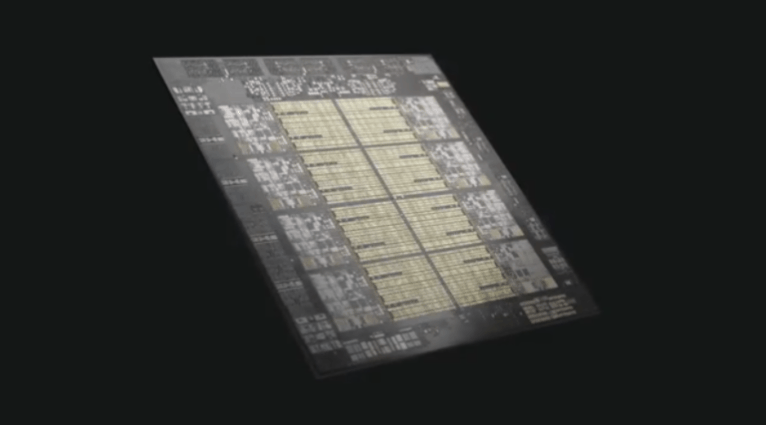
The chip contains eight processor cores with a “deep super-scalar out-of-order instruction pipeline, running with more than 5GHz clock frequency.” With specs like that, the chip is optimized to meet the demands of heterogenous enterprise-level workloads.
The redesigned cache and chip-interconnection infrastructure deliver 32MB cache per core, with room to scale up to 32 Telum chips. The dual-chip module design comes with 22 billion transistors and 19 miles of wire on 17 metal layers.
The chip’s design
The chip was built on 7nm extreme ultraviolet technology created by Samsung and is the first involvement of the IBM Research AI Hardware Center. Telum has been three years in development and will be introduced to a system sometime in the first half of 2022.
Anthony Saporito, a senior technical staff member for IBM Z hardware development, said that the L2 caches can combine to form a virtual 256MB L3 cache. Combining up to eight Telum chips can create a virtual 2GB L4 cache.
Innovating to deliver
Saporito said that one of the key innovations on the Telum design involved building an AI accelerator right onto the silicon.
The team directly connected all of the cores and built an ecosystem up the stack (through hardware design, firmware, and operating systems) and the software that enables the introduction of deep learning into transactions.
Saporito added that to achieve this design, the research and systems group came together to build the directly connected chip for deep learning inferencing that can be deployed at scale. In May, Big Blue’s Research team created a test semiconductor with 2nm fabrication that may improve performance by 45% using the same amount of power or use 75% less energy, compared to 7nm chips. It may go into production towards the end of 2024.