Partners IBM and Samsung Electronics announced the development of a new chip design. By arranging a chip’s transistors in an alternative way, the organizations claim to have a method for producing smartphones with week-long battery lives.
Most organizations with a stake in chip development invest in reducing the size of transistors. The smaller the transistors, the more transistors a chip allows. The more transistors a chip allows, the more effective the chip.
IBM is no exception to the rule. Earlier this year, the organization claimed to have taken a significant step toward the coveted, 2 nanometer (nm) sized transistor. In the same period, Dutch chip manufacturer ASML announced a similar development.
Technology for the production of 2nm transistors fulfils an important requirement for chip improvement. However, several roads lead to Rome, and IBM and Samsung Electronics say they have found one. Their road does not revolve around transistor miniaturization. Instead, it concerns the spatial arrangement of transistors.
The technology
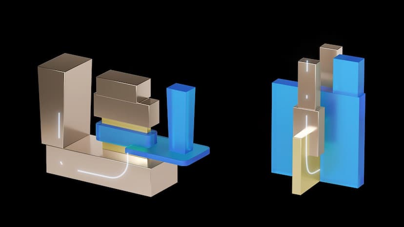
Chip manufacturers such as TSMC and Samsung Electronics currently use a so-called FinFET design, short for ‘fin field-effect transistor’. IBM and Samsung Electronics went public with a VTFET design, short for ‘vertical transport field-effect transistors’.
Samsung and IBM say the VTFET design can deliver twice the power and 85 percent less power consumption than FinFET designs. The reason? “A vertical arrangement of transistors, unlike FinFET.”
The image below outlines the design difference. Although IBM successfully tested the design with the production of concept chips, the organizations do not specify if and when the chips will appear on the market. Nevertheless, the organizations state that VTFET is paving the way to smartphones with battery lives of more than a week and more effective IoT applications for spaceships and self-driving vehicles.