Intel installed the first ASML EUV lithography system for high-performance chip manufacturing at its new Fab 34 facility in Ireland. This will enable the chip giant to produce even smaller chip circuits on a wafer.
The arrival of the EUV lithography system in Ireland should enable the production of the latest-gen Intel 4 chipsets in Europe. Intel and ASML have long collaborated on the development of advanced semiconductor lithography technology. Intel’s Fab 34 production site will be the first plant outside the US to use the new EUV technology.
ASML EUV
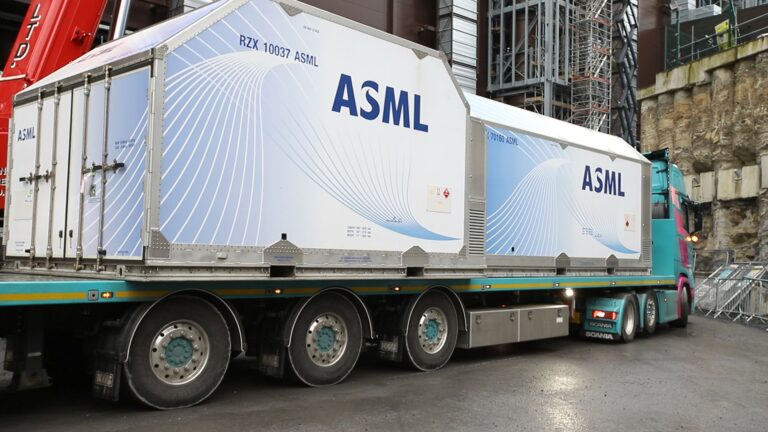
ASML’s EUV machines are so complex and bulky that Intel had to build the Fab 34 facility specifically for this machine. Constructing and prepping the plant took no less than 18 months.

The system consists of 100,000 parts, 3,000 cables, 40,000 bolts and more than a kilometre of tubing. The system features 700 connection points for electrical, mechanical, chemical and gas supplies. It spans four building levels: from the basement, through the subfab, to the factory and with a built-in crane reaching to the ceiling.
The entire machine was flown from Oregon to Ireland in four B747 cargo planes. Meanwhile, 100 specialists from ASML are supervising the installation.
EUV lithography
Lithography scanners are used to print chips onto silicon wafers. In the process, a design template (the so-called ‘reticle’) is scanned. This image is then transferred to a silicon wafer.
EUV lithography allows more transistors on a single chip, making it easier to mass-produce dense chips at lower costs. Generally, the more transistors a chip has, the processing power it delivers.
Tip: ASML achieved record results in 2021, wants to grow further