The designs are the latest in a wide range of Huawei tools related to chip hardware and software.
Huawei has made breakthroughs in electronic design automation (EDA) tools for chips produced at and above 14-nanometre technology. This is according to a report in Reuters, citing a speech by a senior executive and reported in the Chinese financial news outlet Caijing.
According to Caijing, Xu Zhijun, Huawei’s rotating chairman, said in a speech on Feb. 28, that the company will complete testing on the tools this year. The report also noted that Huawei has already developed 78 tools related to chip hardware and software.
“Localisation of EDA tools”
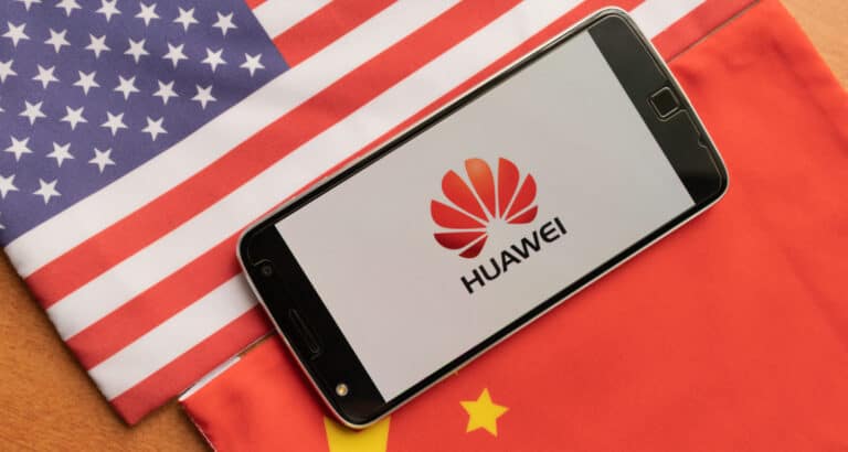
Reuters noted that “the announcement comes as Huawei and other Chinese technology companies rush to localise their supply chains in the face of mounting US sanctions“.
Citing a transcript of Xu’s remarks published by Caijing, Reuters reports Huawei cooperated with domestic EDA companies to create the software, “basically realising the localisation of EDA tools above 14nm.”
Chip design companies use EDA software to produce the blueprints for chips before they become mass manufactured. Chips produced at the 14nm level were first introduced in smartphones in the mid-2010s and are “two to three generations behind leading-edge technology”, Reuters notes.
A bid to get around sanctions
China is home to a handful of domestic EDA software makers, but experts do not consider them globally competitive. The global EDA software market is dominated by three overseas firms, two of which are based in the US – Cadence Design Systems and Synopsys. The third major player is Mentor Graphics, owned by Siemens in Germany. All three companies became subject to Washington’s sanctions against Huawei in 2020.
Due to the US-imposed sanctions regime, Huawei’s chip design division lost access to software and updates needed to design smartphone processors. It also lost access to advanced manufacturing tools at chip production fabs. Huawei was very successful in the smartphone business, it became even bigger than Samsung for a short period of time, but that footprint is almost completely gone.
Localising the EDA tools may help Huawei alleviate some of the effects of the US’s anti-China restrictions.