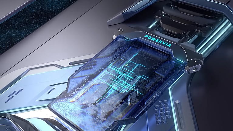
Intel is boasting of its progress with its proprietary PowerVia technology. It is said to be the first chipmaker to create a production-grade test chip with backside power delivery. This would put it two years ahead of the competition.
The Blue Sky Creek chip contains 8 E-cores and runs at 3 GHz. What is unique about this processor is that it no longer has the traditional build of current CPUs. This is based on a structure that runs from small to large when viewed from the bottom: transistors at the bottom, interconnects above and the power supply from the top. However, this structure creates bottlenecks regarding interconnect speeds and power supply stability. This should be a thing of the past with backside power delivery.
From nanometers to Ångström
Anyone who follows the development of processor technology knows that we have seen smaller and smaller process nodes pass by in recent decades. Chip manufacturers constantly compete to get more power on a smaller piece of silicon. Intel seemed to fall behind in this battle, sticking to the 14-nanometer nameplate for its nodes. Compare this to AMD, for example, which had Ryzen chips baked on TSMC processes of 7 and 5 nanometers. However, treating these nodes as if they’re like-for-like is akin to comparing apples to oranges. Just as clock frequency and number of cores do not necessarily tell the whole story, these processes are not directly comparable.
Intel now states that it has moved ahead in the battle for smaller processes, following the “five nodes in four years” ambition expressed by Intel CEO Pat Gelsinger in 2021. PowerVia-tech is at 20 Ångström, or 2 nanometers. According to VP of technology at Intel Ben Sell, the breakthrough is an important milestone. The test chip puts Intel “one process ahead of our competition in bringing backside power delivery to market.” PowerVia is expected to become the force behind Intel’s Arrow Lake generation, scheduled for release in the first half of 2024.
Advantages
Specifically, the test chip should bring about several improvements due to the architectural change. For example, eliminating the front power supply would allow more room for the interconnect layer. There would be 30 per cent less “voltage droop” and a 6 per cent advantage in frequency. Purely in terms of appearance, little changes and there would not even be a problem with heat build-up, despite this build-up being completely new for production chips.
Also read: ‘Intel delays TSMC 3nm chip order’