Samsung Electronics is the world leader in advanced memory and on Monday, the South Korean giant announced it has begun the mass production of the industry’s smallest DRAM (14 nm) based on extreme UV (ultra-violet) technology.
The announcement comes after the company shipped out the industry’s first EUV DRAM in March of 2020. Samsung has increased the number of EUV layers to five to deliver the modern world’s most advanced DRAM process for its DDR5 solutions. Jooyoung Lee, Senior Vice President and Head of DRAM Product & Technology at Samsung Electronics, spoke about the company’s leading position that it has held for close to 30 years.
Samsung promises to continue leading
Lee continued to say that Samsung has been the leader because it is a pioneer in patterning technology innovations. With this new method, Samsung sets yet another technology milestone, with multi-layer EUV that has “enabled extreme miniaturization at 14nm,” a feat not achievable using the conventional argon fluoride process.
Building on this advancement, Lee said the company will continue to provide the most differentiated memory solutions by addressing the need for better performance and capacity in a data-driven world that is getting “5G, AI, and the metaverse.”
Leaps and bounds
DRAM continues to scale down the 10-nm range, bringing EUV technology to the forefront of improving patterning accuracy for greater yields and higher performance. Through the application of five EUV layers to the 14nm DRAM, Samsung has reached the highest bit density while enhancing the overall productivity of the wafer by about 20%.
In addition, the 14nm process can help reduce power consumption by nearly 20% compared to DRAM nodes of the previous generation.
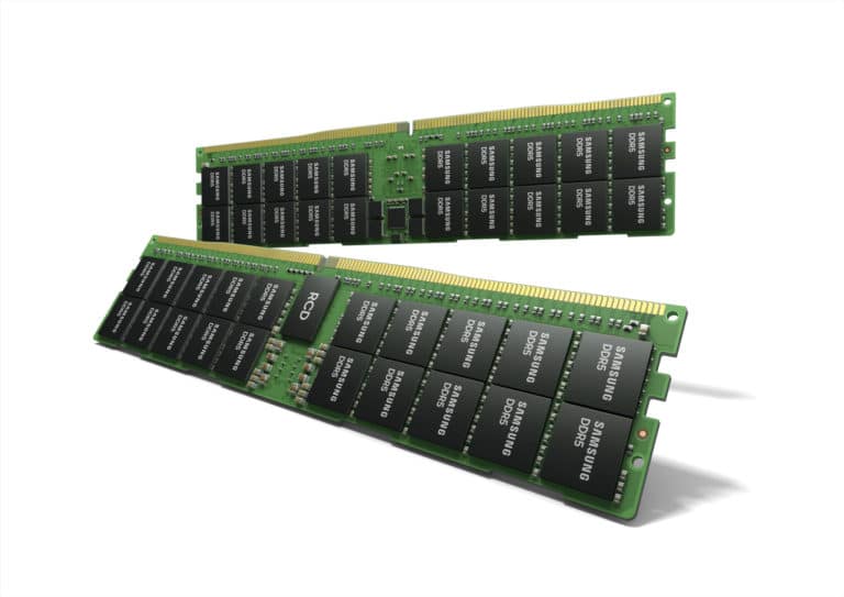
Using the latest DDR5 standard, the 14nm DRAM will unlock high speeds of up to 7.2 gigabits per second, more than twice the speed of DDR4 (3.2Gbps).