Rotterdam-based tech company Nearfield is close to securing an investment of 100 million euros, which it hopes will allow it to expand further. Samsung was one of the first investors in the company and is also loosening the purse strings for this new round. Nearfield provides atomically sharp needles to measure advanced chips without having to touch them.
Where the next location will be is not yet entirely clear. CEO and co-founder Hamed Sadeghian told Dutch financial newspaper FD that Eindhoven could be the location. However, other options are not yet off the table. That is partly due to concerns about sufficient housing for employees and the electricity needed.
The company is headquartered in Rotterdam. In addition, it already has a branch at the High Tech Campus in Eindhoven and one in South Korea, not coincidentally the home of Samsung, its first customer. Additionally, the company has built a clean room near Rotterdam-The Hague Airport.
Checking chips for errors
In recent years, Nearfield has grown into a promising addition to the chip industry in the Netherlands. While companies such as ASML, ASM, and Besi provide the components and equipment that make chip production possible, and others take care of the development of those chips themselves (think NXP), Nearfield provides equipment to measure chips for errors. This is done at the atomic level.
What’s special about Nearfield’s method is that the chips don’t even have to be touched. When testing chips, a manufacturer sometimes has to damage them to test them adequately. With Nearfield’s technology, that is a thing of the past. And that’s quite timely because current quality control measurement techniques are actually no longer adequate for the latest generation of chips, which are getting ever smaller and more complex.
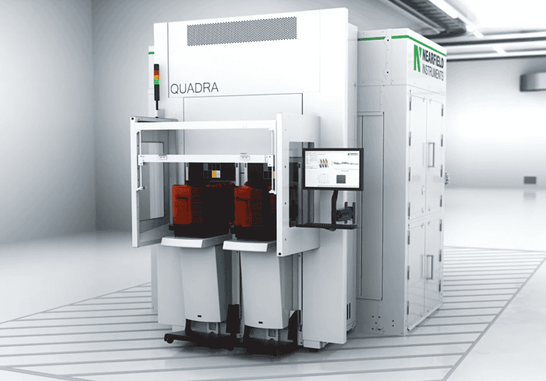
Surface mapping
The method used is called Quadra and involves so-called multi-atomic force inspection (multi-AFM) to map the surface of a chip. Also, to check 3D structures under the visible part of the chip, Nearfield is working on a kind of nano-echoscopy—somewhat similar to ultrasound as it exists in the medical world but much smaller.
Samsung was one of the first investors in 2017, along with venture capitalist Innovation Industries, based in Amsterdam and the High Tech Campus in Eindhoven. ING Bank and Invest-NL, the Dutch government’s investment vehicle, have also poured money in the company.
Samsung recently announced that it has been working with Nearfield for five years. The South Korean company had been using Nearfield’s methods for research purposes for some time. Now, it seems ready to start using them for the production process. Furthermore, all major chip manufacturers, such as Intel and TSMC, are already testing the company’s technology.
The advantage of AFM is that it offers enough detail while being reasonably fast. This contrasts existing techniques such as optical inspection (fast but little detail) or firing electron beams (lots of detail but slow).
Read also: The Netherlands gives NXP, ASML and Nearfield 230 million euro