Nvidia today announced its latest AI GPU: the B200. For the first time, the company is using multiple chips on a single video card for its enterprise hardware.
Nvidia CEO Jensen Huang made this announcement during the keynote of the company’s own GTC event, taking place this week in San Jose. The chip design is codenamed “Blackwell” and is considered the architectural successor to Hopper, which powers the H100 chip. It is built on TSMC’s 4 nanometer process and is twice the physical size of its predecessor. The promised speed improvement of the B200 (a set of two B100 dies) versus the H100 is 30x, with Huang focusing specifically on AI inferencing (the generation of information by LLMs).
Blackwell ecosystem
This new “AI superchip” contains 208 billion transistors. However, Huang’s emphasis was not so much on the processor itself, but on the scalability of the new architecture. Thus, companies with a number of H100 chips can replace them within existing form factors with the B200. One variant the Nvidia CEO showed included two B200s (themselves a set of twin chip dies packaged together) and a Grace CPU. The HBM3e memory is accessible by all parts of the hardware, so its split nature should not introduce latency.
Beyond the specifications themselves, Nvidia has introduced a number of new features. For example, the new chip can simplify certain AI calculations whenever possible on the fly, making AI training significantly faster than before. It’s an important step, as the training process of LLMs can take several weeks, thereby curtailing innovation in AI. The so-called “RAS engine” functions as a security check that acts as an “on-board tester” for the AI calculations. In addition, security options provide the ability to encrypt data at rest, in transit and during calculations.
Tip: Will Groq depose Nvidia from its AI throne with the LPU?
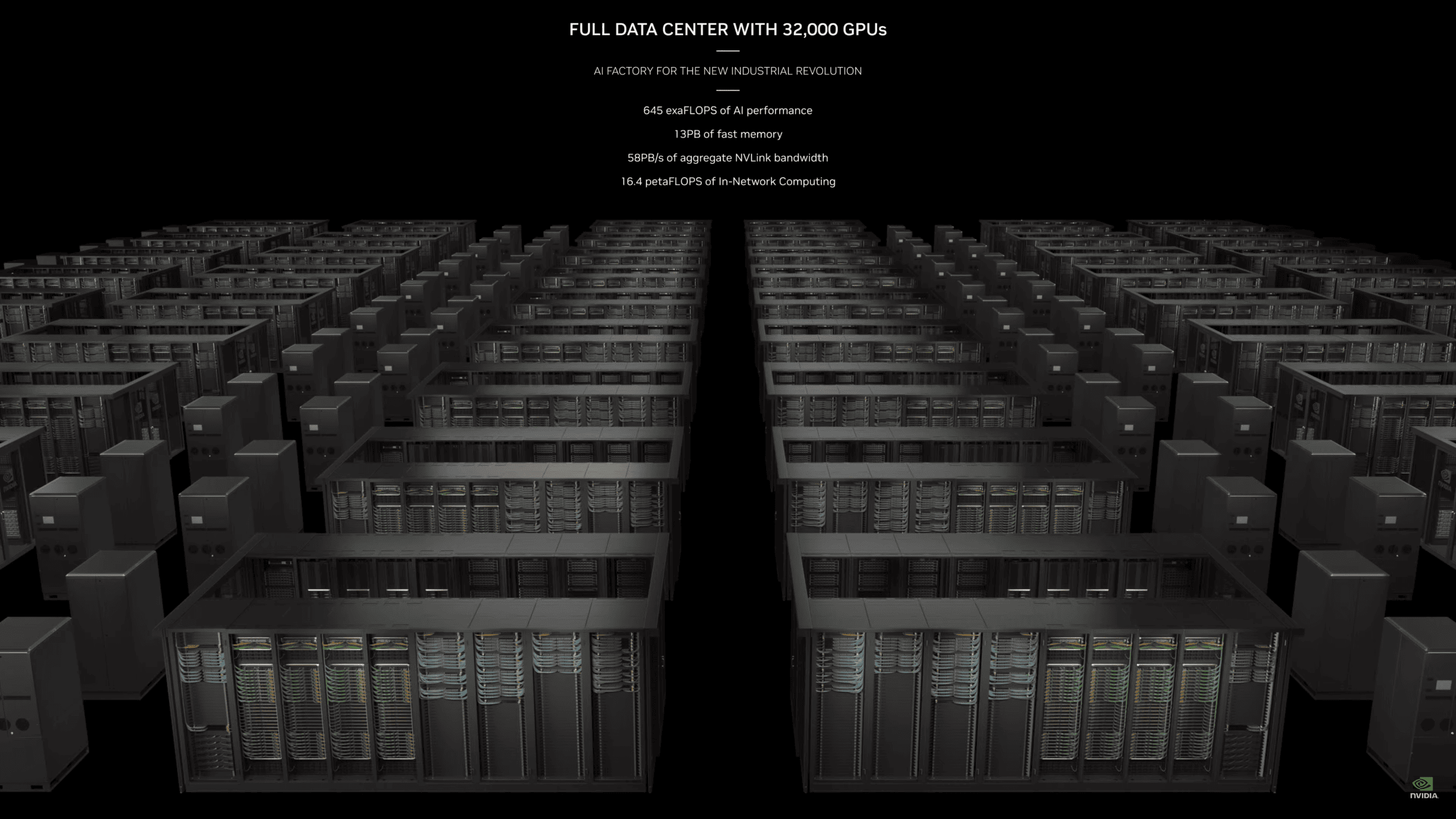
A new NVLink Switch chip allows multiple B200s to communicate with each other as if they were a single GPU. In a DGX system, it delivers 22x the training speed of a single H100 and 45x the inferencing speed. It requires 2 liters of fluid per second and heats it from 25 degrees Celsius to 45 degrees, which betrays a significant need for continuous heat dissipation. Because the number of GPUs required for the same computing power as before is a lot smaller, Huang argues that training new AI models will be significantly more economical than it has been so far.
Emphasis on accelerated computing
An important term Huang used during the GTC keynote was accelerated computing. General computing has had its day, ‘accelerated computing’ is the future, Nvidia’s CEO suggested. It is a common term amongst Huang’s presentation, and it indicates that specific workloads require more than just a powerful CPU. GPUs with tens of thousands of cores can process AI calculations at lightning speed; it is the reason that Nvidia, not Intel, AMD or any other major vendor, has been able to benefit so much from the sudden rise of GenAI.
And availability?
It remains to be seen whether Nvidia can meet the huge demand of these AI chips. Because of TSMC’s advanced packaging technology, the yield rate, or the percentage of chips that meet the stringent hardware requirements after they are produced, is not immediately to be expected to be all that high. However, everything seems to give way to the fastest AI acceleration currently possible.
The announcement of the Blackwell comes at a particularly early stage. After all, the refresh to the H100, the H200, and the so-called GH200 “Superchip” have yet to appear.
Also emphasis on software
During the GTC keynote, Huang also paid a great deal of attention to software development. In that area, among other things, Nvidia is trying to drive adoption of its Omniverse, a cloud platform aimed at developing, deploying and managing 3D applications. That platform should enable the building of digital twins, with Nvidia citing (renewed) partnerships from Ansys, Synopsys and Cadence.
Also read: H200: Nvidia’s latest AI chip with 141GB of super-fast memory