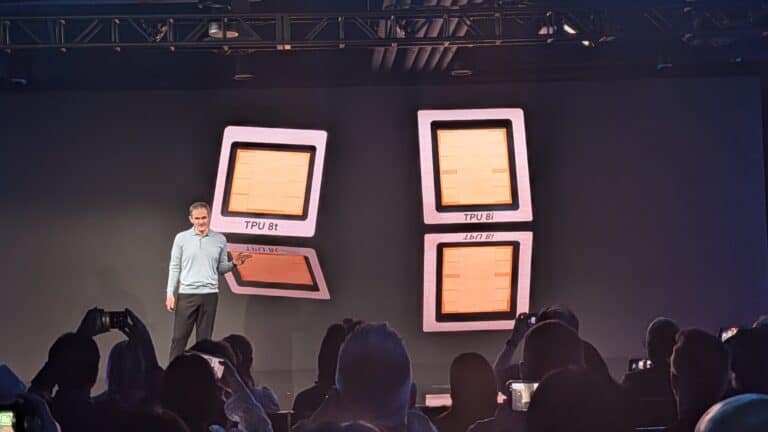
At Google Cloud Next 2026 in Las Vegas the company presents its 8th-generation TPUs. For the first time it introduced two TPUs simultaneously, separating inference and training. The TPU 8t and TPU 8i have been completely redesigned, each for a fundamentally different purpose. Google has once again made a huge leap forward in performance and efficiency. It now offers an alternative infrastructure to Nvidia. The big question is whether it can convince organizations to choose Google’s AI infrastructure.
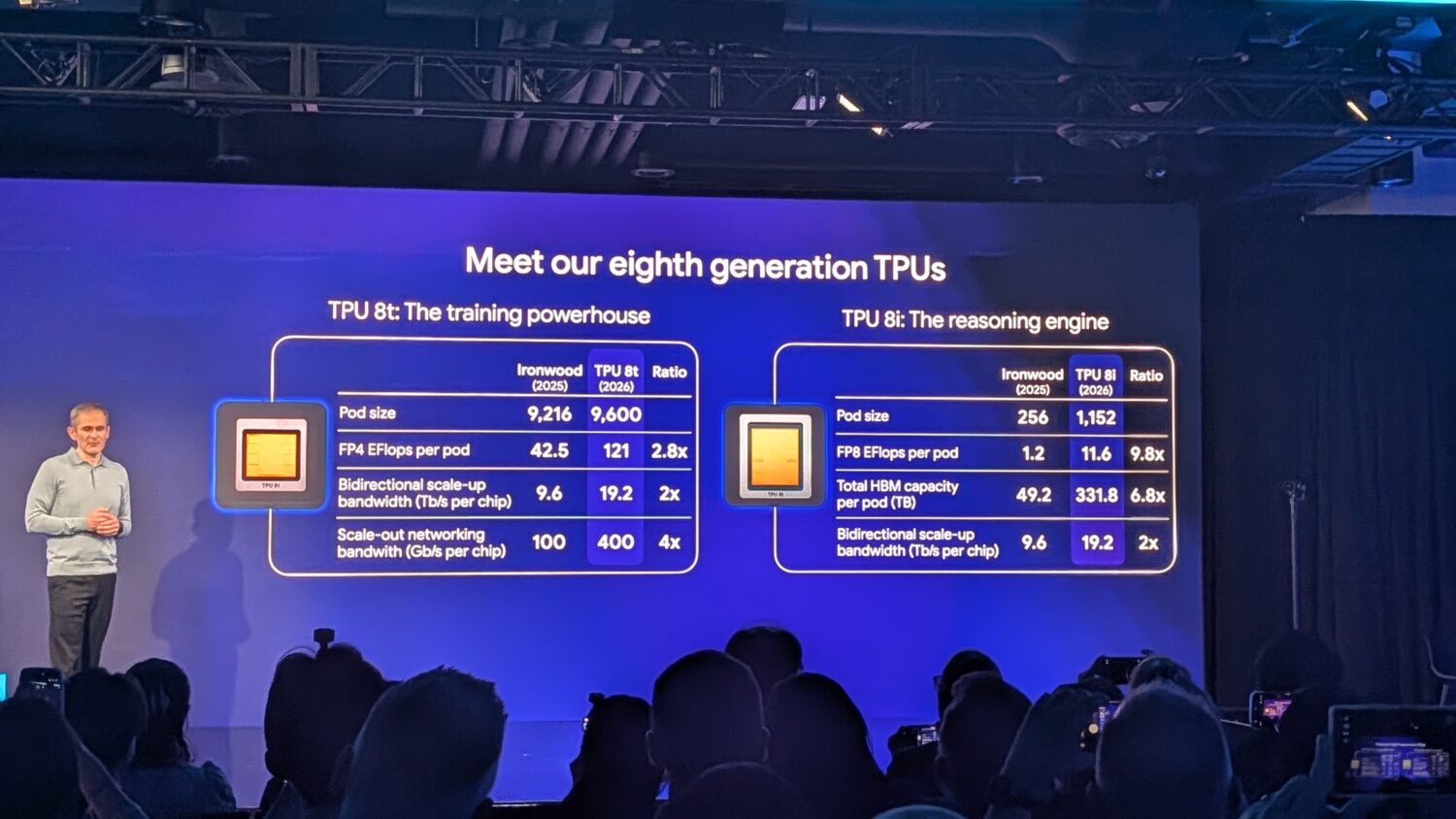
A year ago, Google stood on the same stage in Las Vegas to present Ironwood, the seventh-generation TPU that was Google’s most powerful AI chip at the time. Ironwood was already a significant step forward with up to 42.5 exaflops per pod and 192 GB of HBM per chip. Google already spoke about a focus on inference. Now, a year later, Google is presenting two successors.
Two chips, each with its own purpose
The rationale behind this split is logical. Training and inference are fundamentally different workloads with different requirements. Training demands maximum computing power, massive scalability, and high bandwidth. Inference, on the other hand, requires low latency (especially with AI agents), more HBM capacity per pod, and efficient real-time communication between large numbers of chips. That is why Google is switching to a strategy with separate chips for Training and Inference. These have become the TPU 8t and 8i, where the t stands for training and the i for inference.
TPU 8t: the training beast
The TPU 8t is built for one thing: training frontier models as quickly as possible. Google claims that this can reduce the development cycle for large models from months to weeks. The figures support that ambition.
A single TPU 8t superpod can now contain 9,600 chips, which is comparable to Ironwood; however, this new superpod delivers nearly three times as much computing power: 121 exaflops. The pod’s total memory pool amounts to two petabytes of HBM, with twice the inter-chip bandwidth of the previous generation.
Notable is the introduction of the Virgo Network: Google’s new scale-out fabric that allows the TPU 8t to scale up to 134,000 chips in a single fabric within a single data center, and up to one million chips in a training cluster spanning multiple data centers. This is not a theoretical limit for the future, but the architecture upon which Google’s own model training capacity will be built in the coming years.
In addition to the enormous computing power, there is also a focus on reliability. The TPU 8t is designed for over 97% so-called “goodput”: the ratio of productive computing time to total uptime. When training models, every second or every percentage point counts, because one percent less often means days of additional training time. The Virgo Network is also designed to automatically detect and resolve failures by leveraging real-time telemetry across tens of thousands of chips. This includes automatic rerouting in the event of defective chips or broken connections. The network automatically reconfigures itself without human intervention while model training continues uninterrupted.
TPU 8i: the inference chip
The TPU 8i is ultimately the more interesting of the two, because most organizations don’t train models, they use them. To use an AI model, you need an inference chip, such as the TPU 8i. The shift from standalone models to AI agents that communicate with each other and perform tasks is driving much higher demand for inference.
This is also reflected in the pod configuration of the TPU 8i. Instead of 256 chips in Ironwood, a single pod can now hold 1,152 chips. This allows a single TPU 8i pod to deliver enormous computing power.

Google has addressed several specific issues that hindered performance during inference at scale:
The TPU 8i features more HBM memory than its predecessor, with 288 GB of HBM combined with 384 MB of on-chip SRAM. This allows a larger workload to be stored in memory, reducing latency.
The number of physical CPU hosts per server has doubled, providing greater CPU support and enabling workloads to run even faster. To achieve this, Google is also switching to its own Axion ARM processors, which work very well with Google’s own TPUs.
Latency has been further reduced by doubling the chip-to-chip bandwidth to 19.2 Tb/s and by reducing the network diameter by 50%. This is what Google calls the Boardfly architecture.
All in all, this new chip delivers greater computing power and efficiency while reducing power consumption. Google claims twice the performance per watt and cites an 80 percent better price-performance ratio compared to Ironwood.
Also read: Google Cloud accelerates AI development with new TPUs and VMs
Google builds a full stack
What sets Google apart from the rest of the industry is not a single chip or AI model, but the integration between all components, from the silicon, network, and data center to the power supply, software, and AI models. Because Google manages everything in-house, it can better coordinate all elements and achieve higher performance.
More is needed to convince organizations. Google notes that there is broad software support; JAX, MaxText, PyTorch, SGLang, and vLLM are natively supported. Bare-metal access is available, meaning customers get direct hardware access without the overhead of virtualization. Google’s chips aren’t available separately, only through Google Cloud, so if your organization chooses this, you’re effectively locked in.
Google does support the well-known software tools that are also widely used with Nvidia chips, for example, but once you step into the Google infrastructure with all the tooling the company provides, the likelihood of switching to an Nvidia infrastructure is significantly lower. That would ultimately require many adjustments.
Availability
Both chips will become generally available via Google Cloud later this year. Google has not yet announced an exact date. The chips have been in development for two years, and Google plans to deploy them internally on a larger scale for its own services and, of course, its own model training.
The performance gains are impressive; every year, Google manages to get more out of its own chips. Google develops the chips for its own use and for commercial use in Google Cloud. Google can already use a significant number of the chips itself; the question is whether it will also be able to generate strong customer interest in the new chips and the associated infrastructure. Some organizations fear lock-in; with Nvidia chips, you’re tied to Nvidia, but you can still purchase the platform and servers elsewhere and deploy them in your own data center.